logo
米国について
あなたのプロフェッショナルで信頼できるパートナーです
上海の有名な貿易CO.、株式会社は中国最もよい市である、私達の工場は2014年にウーシー都市で創設されます上海市に置き。 私達は電子工学、光学、光電子工学および他の多くの分野で広く利用されたウエファー、基質およびcustiomized光学ガラスparts.componentsにいろいろな材料を処理することを専門にします。私達はまた多くの国内を密接に使用して、海外大学、研究所および会社はR & Dのプロジェクトに、カスタマイズされた製品とサービスを提供します。 それは私達のよいreputatiaonsによって私達のすべての顧客との協同のよい関係の維持へ私達の視野です。...
もっと学びなさい

0

確立される年

0

数百万+
年間売上
中国 SHANGHAI FAMOUS TRADE CO.,LTD 高品質
信頼証券 信用チェック RoSH サプライヤーの能力評価 企業には厳格な品質管理システムと 専門的なテストラボがあります
中国 SHANGHAI FAMOUS TRADE CO.,LTD 開発
専門的な設計チームと 先進的な機械のワークショップ 必要な製品を開発するために協力することができます.
中国 SHANGHAI FAMOUS TRADE CO.,LTD 製造業
先進的な自動機械 厳格なプロセス制御システム 電気端末を全て 製造できます
中国 SHANGHAI FAMOUS TRADE CO.,LTD 100%のサービス
卸売品と小型のパッケージは FOB,CIF,DDU,DDPです 心配事項の最善の解決策を 見つけられるようにしましょう.

質 ガリウム窒化物のウエファー & サファイアのウエファー メーカー

自分 の 要求 に より 適した 製品 を 探す.
事件とニュース
最新 の 熱帯 地点
ZMSH事例研究:高品質の合成色のサファイアを供給する主要企業
ZMSH事例研究:高品質の合成色のサファイアを供給する主要企業     紹介ZMSHは合成宝石業界で 有名な名前で 高品質で鮮やかな色のサファイアを 幅広い範囲で提供しています私たちの提供には,王室ブルーのような色パレートの幅があります鮮やかな赤,黄色,ピンク,ピンクオレンジ,紫色,そしてエメラルドとオリーブ緑色を含む複数の緑色信頼性の高い技術を必要としている企業にとって視覚的に目立つ 耐久性のある合成宝石です 合成 宝石 を 強調 するZMSHの製品ラインナップの中心は 合成サファイアで 自然の宝石の輝きと質を模倣し 多くの利点を提供していますこのサファイアは,色調の一貫性と耐久性を得るために慎重に製造されています.自然に生じる石に優れている代替品です 人工 の ザファイア 石 を 選ぶ こと の 益 卓越 し た 一貫性: 私たちの実験室で作られたサファイアは 厳格な品質基準を満たす 制御条件下で生産されています.採掘された宝石にしばしば見られる色と透明性の変化から自由です. 広い 色 の 選択ピンクやピンクオレンジのような柔らかい色も提供しています. 緑色からオリーブ色まで,特定の顧客要求に応えるように調整されたこの色と色調の柔軟性により デザインや産業用途に最適です 安価 な 価格: 実験室で栽培されたサファイアは,視覚的魅力や構造的整合性を犠牲にせずに,より予算に優しい代替品です.天然石のコストのほんの一部で高品質の宝石を必要とする顧客に優れた価値を提供します贅沢品と実用的な用途の両方に最適です 環境 と 倫理 に 配慮 する: 合成宝石を選択することで,顧客は,伝統的な宝石採掘とよく関連する環境被害と倫理上の懸念を回避できます.ZMSHの合成サファイアは 環境に配慮した方法で作られています持続可能で責任ある選択を提供します 強さ と 柔軟性: 合成 ザファイア は,天然 の ザファイア と 同じ 硬さ を 持っ ており,高級 宝石 から 工業 級 の 宝石 まで の 様々な 用法 に 最適 です.硬さ 9 モーススケールこの宝石はあらゆる環境で長持ちします   結論ZMSHは最高級の合成色のサファイアを提供することに専念し,顧客にカスタマイズ可能でコスト効率の良い持続可能な宝石ソリューションを提供しています.エレガントなアクセサリーのために王室ブルーを探しているかどうか工業用部品のエメラルド緑色,または他の目立つ色,ZMSHは美しさ,一貫性,強さを組み合わせる宝石を提供します.合成サファイアを生産する専門知識により,様々な産業のニーズを満たすことができます信頼性の高い品質と倫理的慣行を保証します.
ケーススタディ:新しい4H/6H-P 3C-N SiC 基板でZMSHの突破
紹介 
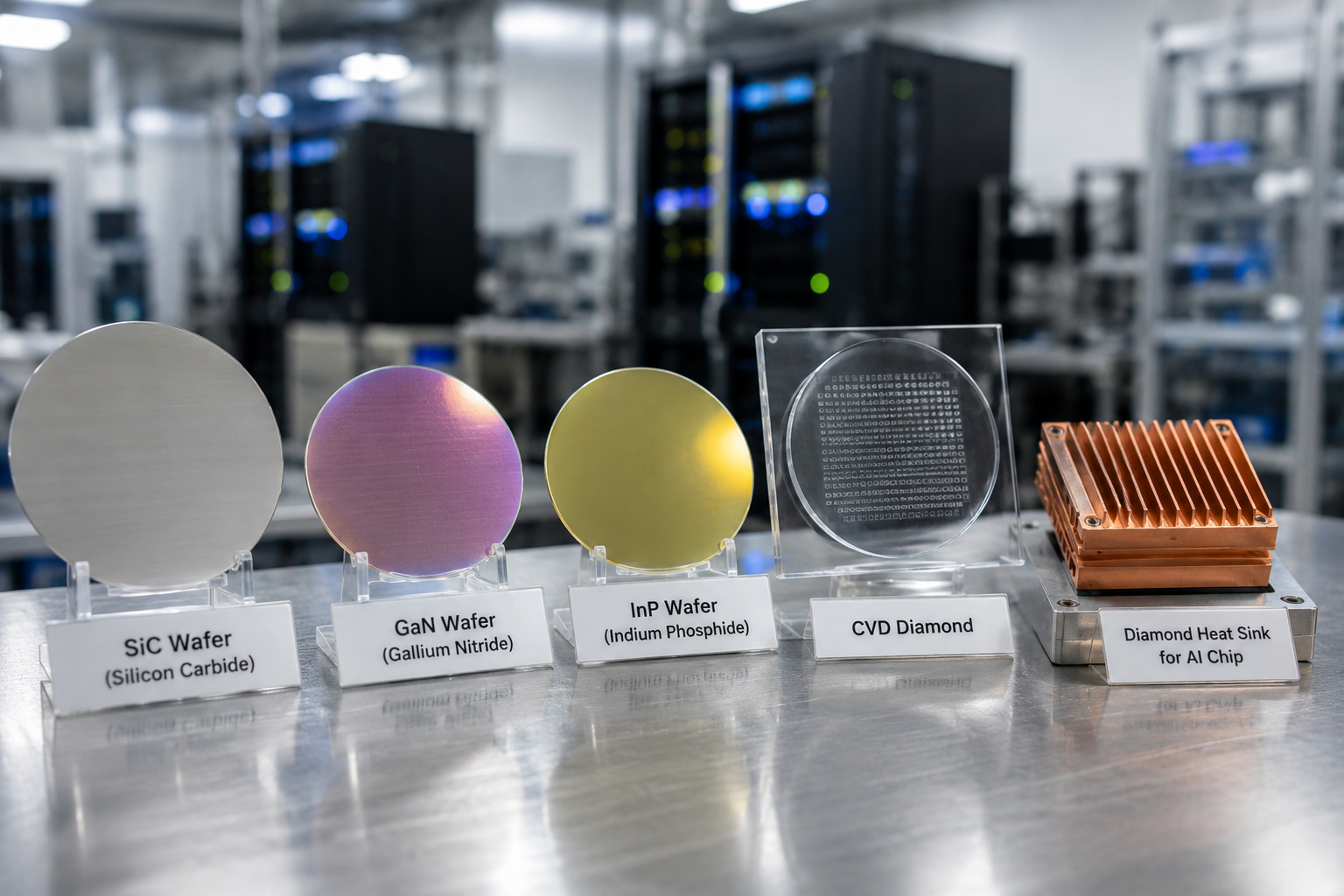
ZMSHは一貫して,高性能を提供することで知られるシリコンカービッド (SiC) ウェーバーと基板の革新の最前線に立っています6H-SiCそして4H-SiC高性能および高周波アプリケーションにおける より優れた材料に対する需要の増大に対応するためZMSHは,製品提供を拡大し,4H/6H-P 3C-N SiCこの新しい製品は,従来の材料を組み合わせることで重要な技術的飛躍を遂げています.4H/6Hポリタイプ SiC革新的な基板3C-N SiC次の世代機器の性能と効率の新たなレベルを提供します. 既存の製品概要: 6H-SiCと4H-SiC基板 主要 な 特徴 結晶構造: 6H-SiCと4H-SiCの両方が六角形結晶構造を有する. 6H-SiCは電子移動性がわずかに低く,帯域が狭い.4H-SiCは,より高い電子移動性と,より広いバンドギャップを誇っています..2 eVで,高周波,高電力用途に適している. 電気伝導性: N型と半絶縁のオプションの両方で利用可能で,さまざまなデバイスニーズに柔軟性があります. 熱伝導性: これらの基板は,高温環境における熱を散布するために不可欠な3.2〜4.9W/cm·Kの熱伝導性を示しています. 
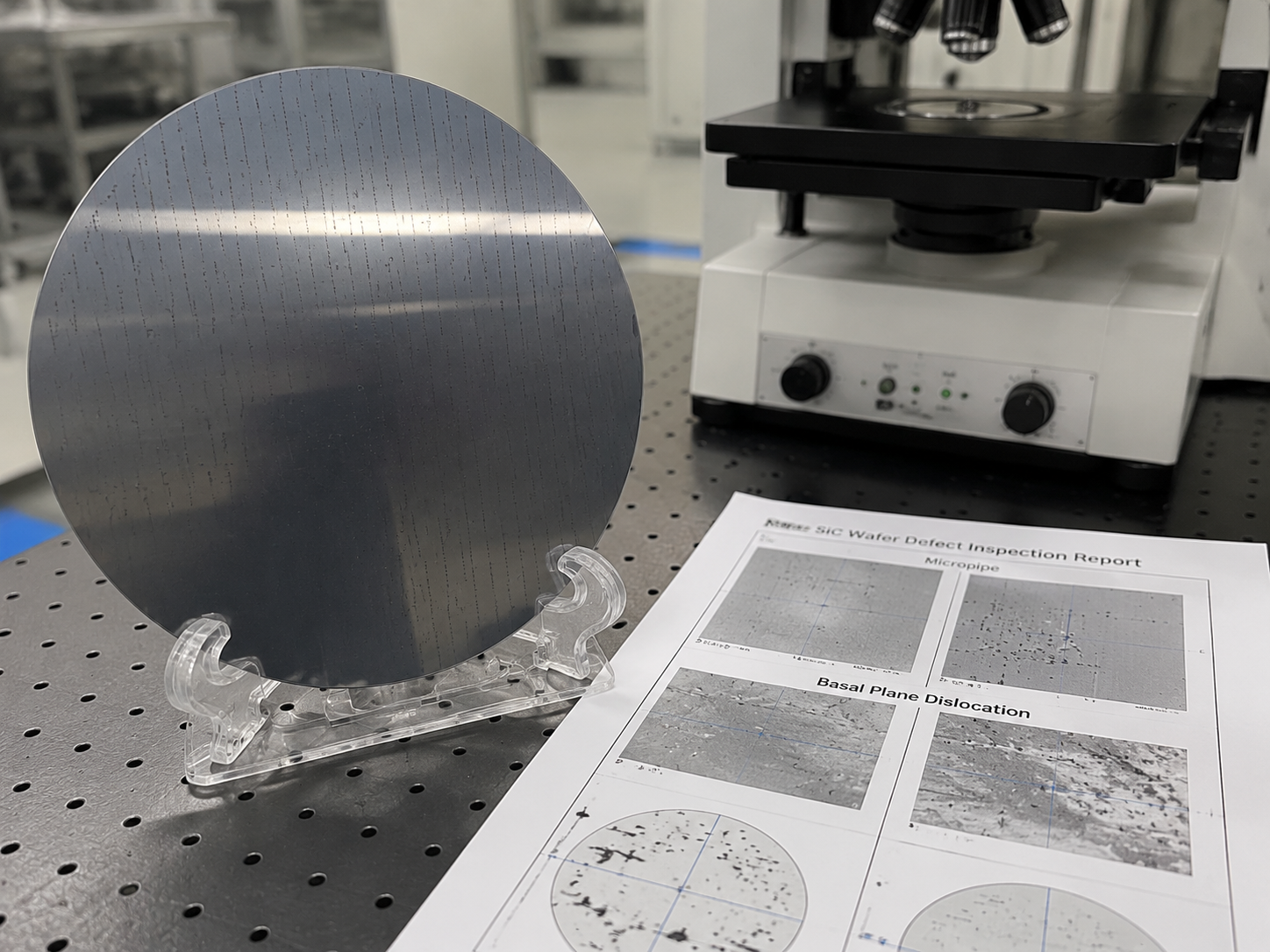
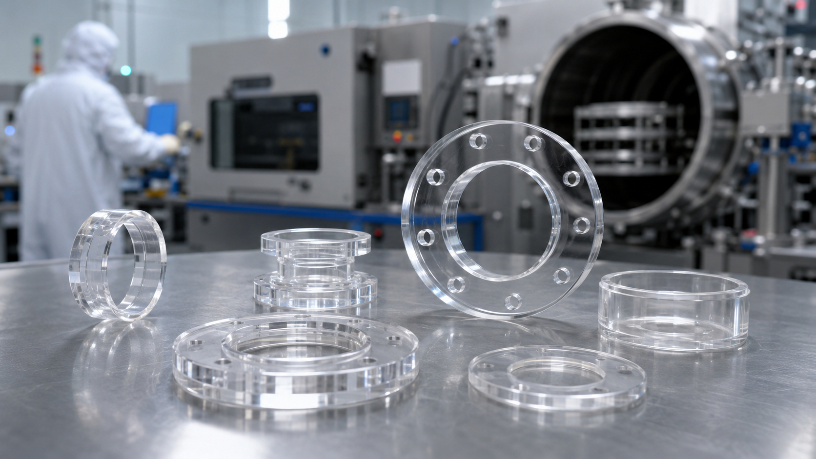
メカニカル 強さ: 基板はモース硬度9を持っています.2要求の高いアプリケーションで使用するための強さと耐久性を提供します. 典型的な用途: パワーエレクトロニクス,高周波装置,高温や放射線に耐える環境で使用される. 課題その間6H-SiCそして4H-SiC高性能,高温,高周波のシナリオでは 特定の制限に直面します 欠陥率,電子移動性の制限,次の世代のアプリケーションの有効性を制限します市場では,より高い運用効率を確保するために,性能が向上し,欠陥が少なくなる材料がますます必要になっています. 新しい製品革新: 4H/6H-P 3C-N SiC基板 ZMSHは,以前のSiC基板の限界を克服するために,4H/6H-P 3C-N SiCこの新しい製品はエピタキシアル成長3C-N SiCフィルム4H/6Hポリタイプ基板電子と機械の性能を向上させる. 重要な 技術 的 改善 
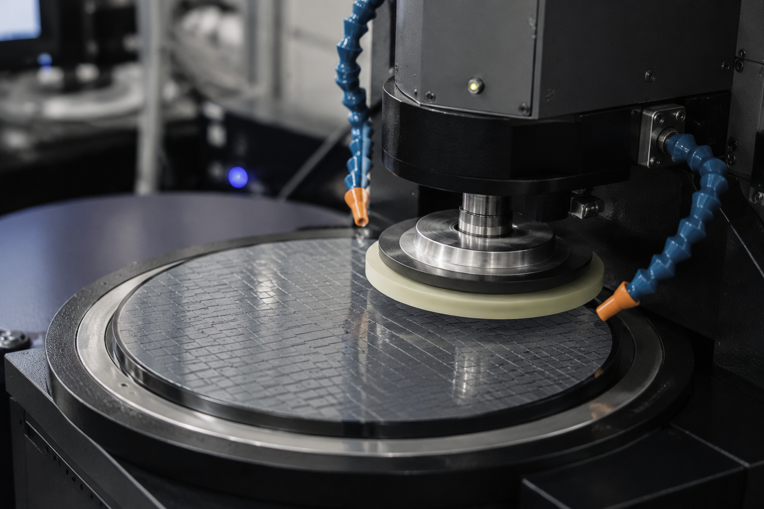
ポリタイプとフィルム統合について3C-SiCフィルムは,表頭軸で栽培されます.化学蒸気堆積 (CVD)について4H/6H基質, 格子不一致と欠陥密度を大幅に削減し,材料の整合性を改善します. 電子 の 移動 性 を 強化 するについて3C-SiCフィルムは従来のフィルムと比較して優れた電子移動性を有します4H/6H基質高周波アプリケーションに最適です 改善された断断電電圧: 試験により,新しい基板はかなり高い断熱電圧を提供しており,電力密度の高いアプリケーションに適しています. 
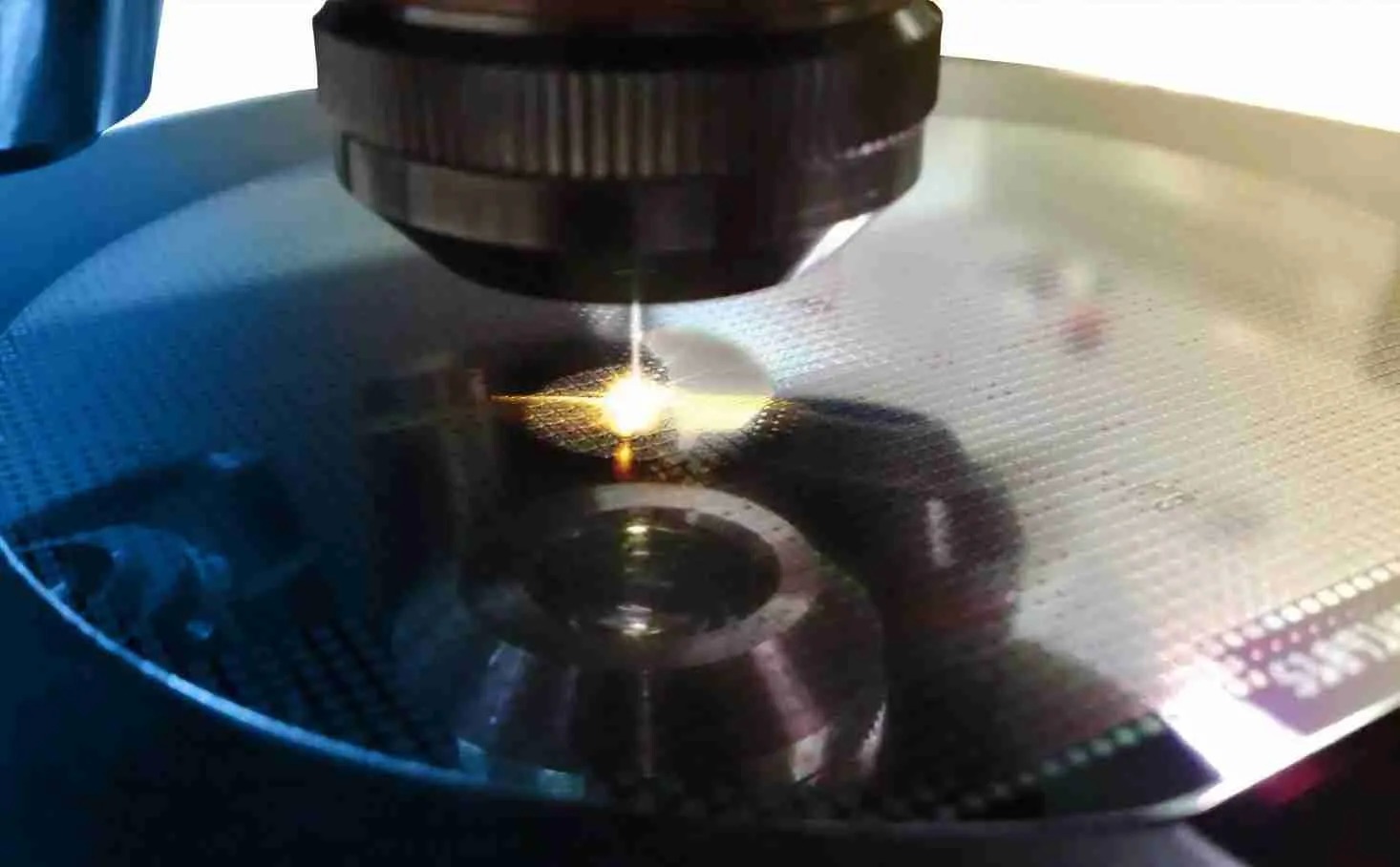
欠陥の減少:最適化された成長技術により,結晶の欠陥と外位を最小限に抑え,困難な環境で長期にわたる安定性を保証します. 光電子能力: 3C-SiCフィルムはまた,紫外線検出器や他の様々な光電子アプリケーションに特に有用なユニークな光電子特性を導入します. 新しい4H/6H-P 3C-N SiC基板の利点 電子の移動性と分解強度が高くなるについて3C-N SiCフィルムは高性能高周波装置で優れた安定性と効率性を保証し,より長い使用寿命とより高い性能をもたらします. 熱伝導性 と 安定性 を 向上 さ せる: 熱を散らす能力が向上し,高温 (1000°C以上) の安定性により,基板は高温用途に適しています. 拡張された光電子アプリケーション: 基板の光電子特性により,その応用範囲が拡大し,紫外線センサーやその他の先進光電子装置に最適化されています. 化学 的 に 耐久 性 を 高める: 新しい基板は化学腐食と酸化に強い耐性を有し,厳しい産業環境での使用には不可欠です. 応用分野 について4H/6H-P 3C-N SiCこの基板は,高度な電気,熱,光電子特性により,幅広い最先端アプリケーションに最適です. 電力電子機器超高断熱電圧と熱管理により,MOSFET,IGBTそしてスコットキーダイオード. RF とマイクロ波装置: 高い電子移動性は,高周波での卓越した性能を保証しますRFそしてマイクロ波装置. 紫外線検出器と光電子機器■ 光電子特性は3C-SiC特別に適しているように紫外線検出そして様々な光電子センサー 結論と製品推奨 ZMSHは4H/6H-P 3C-N SiCこの革新的な製品は,電子移動性が向上し,欠陥密度が低下し,改善された断熱電圧電力,周波数,光電子市場の需要を満たすのに適しています.極端な条件下での長期間の安定性も,さまざまなアプリケーションのための非常に信頼性の高い選択になります. ZMSHは顧客に4H/6H-P 3C-N SiCその最先端の性能能力を活用する基板ですこの製品は,次世代のデバイスの厳しい要求を満たすだけでなく,迅速に進化する市場で顧客に競争優位性を得るのに役立ちます.   製品推奨   4インチ 3C N型 SiC基板 シリコンカービッド基板 厚さ 350um プライムグレード ダミーグレード       - デザインアートワークでカスタマイズされたものをサポートします   - 3C SiC の立方結晶で,SiC モノ結晶で作られています.   - 高硬度 モース硬度9まで2ダイヤモンドに次ぐ   - 高温環境に適した優れた熱伝導性   - 高周波,高電力電子機器に適した広い帯域特性が有する.
Comprehensive Overview of Advanced Ceramics Used in Semiconductor Equipment
Comprehensive Overview of Advanced Ceramics Used in Semiconductor Equipment   Precision ceramic components are essential elements in core equipment for key semiconductor manufacturing processes such as photolithography, etching, thin film deposition, ion implantation, and CMP. These parts—including bearings, guide rails, chamber liners, electrostatic chucks, and robotic arms—are especially critical inside process chambers, where they serve functions such as support, protection, and flow control. This article provides a systematic overview of how precision ceramics are applied in major semiconductor fabrication equipment.       Front-End Processes: Precision Ceramics in Wafer Fabrication Equipment 1. Photolithography Equipment   To ensure high process accuracy in advanced photolithography systems, a wide range of ceramic components with excellent multifunctionality, structural stability, thermal resistance, and dimensional precision are used. These include electrostatic chucks, vacuum chucks, blocks, water-cooled magnet bases, reflectors, guide rails, stages, and mask holders.   Key ceramic components: Electrostatic chuck, motion stage   Main materials:Electrostatic chucks: Alumina (Al₂O₃), Silicon Nitride (Si₃N₄), Motion stages: Cordierite ceramics, Silicon Carbide (SiC)   Technical challenges: Complex structure design, raw material control and sintering, temperature management, and ultra-precision machining. The material system of lithography motion stages is crucial for achieving high accuracy and scanning speed. Materials must feature high specific stiffness and low thermal expansion to withstand high-speed movements with minimal distortion—thus improving throughput and maintaining precision.       2. Etching Equipment   Etching is critical for transferring circuit patterns from the mask to the wafer. Key ceramic components used in etching tools include the chamber, viewport window, gas distribution plate, nozzles, insulator rings, cover plates, focus rings, and electrostatic chucks. Key ceramic components: Electrostatic chuck, focus ring, gas distribution plate   Main ceramic materials: Quartz, SiC, AlN, Al₂O₃, Si₃N₄, Y₂O₃     Etching Chamber: With shrinking device geometries, stricter contamination controls are required. Ceramics are preferred over metals to prevent particle and metal ion contamination.     Material requirements: High purity, minimal metal contamination Chemically inert, especially to halogen-based etching gases High density, minimal porosity Fine grain, low grain boundary content Good mechanical machinability Specific electrical or thermal properties if needed   Gas Distribution Plate: Featuring hundreds or thousands of precision-drilled microholes, these plates uniformly distribute process gases, ensuring consistent deposition/etching.   Challenges: Demands on hole diameter uniformity and burr-free inner walls are extremely high. Even slight deviations can cause film thickness variation and yield loss.   Main materials: CVD SiC, Alumina, Silicon Nitride   Focus Ring: Designed to balance plasma uniformity and match the conductivity of the silicon wafer. Compared to traditional conductive silicon (which reacts with fluorine plasma to form volatile SiF₄), SiC offers similar conductivity and superior plasma resistance, enabling longer life.   Material: Silicon Carbide (SiC) ​       3. Thin Film Deposition Equipment (CVD / PVD)     In CVD and PVD systems, key ceramic parts include electrostatic chucks, gas distribution plates, heaters, and chamber liners. Key ceramic components: Electrostatic chuck, ceramic heater   Main materials: Heaters: Aluminum Nitride (AlN), Alumina (Al₂O₃)   Ceramic Heater: A critical component located inside the process chamber, directly in contact with the wafer. It supports the wafer and ensures uniform, stable process temperatures across its surface. ​   Back-End Processes: Precision Ceramics in Packaging & Testing Equipment       1. CMP (Chemical Mechanical Planarization) CMP equipment utilizes ceramic polishing plates, handling arms, alignment platforms, and vacuum chucks for high-precision surface planarization.   2. Wafer Dicing and Packaging Equipment Key ceramic components: Dicing Blades: Diamond-ceramic composites, cutting speed ~300 mm/s, edge chipping

2025

07/02

How does stress develop in quartz materials?
How does stress develop in quartz materials?     1. Thermal Stress During Cooling (Primary Cause) Quartz glass develops internal stress when exposed to non-uniform temperatures. At any given temperature, quartz glass exhibits a specific atomic structure that is most "suitable" or stable under those thermal conditions. The spacing between atoms changes with temperature—this is known as thermal expansion. When quartz glass experiences uneven heating or cooling, differential expansion occurs.   Stress typically arises when hotter regions attempt to expand but are constrained by surrounding cooler areas. This results in compressive stress, which usually does not damage the product. If the temperature is high enough to soften the quartz glass, the stress may be relieved. However, if the cooling process is too rapid, the viscosity of the material increases too quickly, and the atomic structure cannot adjust in time to accommodate the temperature drop. This leads to the formation of tensile stress, which is more likely to cause structural damage.   Stress increases progressively as the temperature drops and can reach high levels after cooling ends. In fact, when the viscosity of quartz glass exceeds 10^4.6 poise, the temperature is referred to as the strain point—at this stage, the viscosity is too high for stress relaxation to occur.     Normal>Deformed>           2. Stress from Phase Transition and Structural Relaxation   Metastable Structural Relaxation: In the molten state, quartz exhibits a highly disordered atomic arrangement. During cooling, atoms attempt to transition toward a more stable configuration. However, due to the high viscosity of the glassy state, atomic movement is limited, leaving the structure in a metastable state. This generates relaxation stress, which may be slowly released over time (as observed in the aging phenomenon in glasses).   Microscopic Crystallization Tendency: If molten quartz is held at specific temperature ranges (e.g., near the devitrification temperature), microscopic crystallization may occur (e.g., precipitation of cristobalite microcrystals). The volume mismatch between crystalline and amorphous phases can induce phase transition stress.       3. External Loads and Mechanical Actions 1) Stress Induced During Machining Mechanical processing such as cutting, grinding, and polishing can introduce surface lattice distortion, resulting in machining stress. For example, cutting with a grinding wheel generates localized heat and mechanical pressure at the edge, leading to stress concentration. Improper techniques during drilling or slotting can create notches that act as crack initiation sites.   2) Load Stress in Service Environments When used as a structural material, fused quartz may bear mechanical loads such as pressure or bending, generating macroscopic stress. For instance, quartz containers holding heavy substances develop bending stress.       4. Thermal Shock and Sudden Temperature Changes 1) Instantaneous Stress from Rapid Heating or Cooling Although fused quartz has an extremely low coefficient of thermal expansion (~0.5×10⁻⁶/°C), rapid temperature changes (e.g., heating from room temperature to high temperatures or immersion in ice water) can result in localized thermal expansion or contraction, causing instantaneous thermal stress. Laboratory glassware made of quartz may fracture under such thermal shocks. 2) Cyclic Temperature Fluctuations Under long-term cyclic thermal environments (e.g., furnace linings or high-temperature optical windows), repeated thermal expansion and contraction can accumulate fatigue stress, accelerating material aging and cracking.           5. Chemical Effects and Stress Coupling 1) Corrosion and Dissolution Stress When fused quartz comes into contact with strong alkaline solutions (e.g., NaOH) or high-temperature acidic gases (e.g., HF), its surface may undergo chemical corrosion or dissolution, disrupting structural uniformity and causing chemical stress. Alkaline attack can cause surface volume changes or form microcracks. 2) CVD-Induced Stress In chemical vapor deposition (CVD) processes, coating quartz with materials like SiC may introduce interfacial stress due to mismatches in thermal expansion coefficients or elastic moduli between the film and the substrate. Upon cooling, such stress may cause film delamination or substrate cracking.     6. Internal Defects and Impurities 1) Bubbles and Embedded Impurities During melting, residual gas bubbles or impurities (e.g., metal ions or unmelted particles) may become trapped in fused quartz. The difference in physical properties (e.g., thermal expansion coefficient or modulus) between these inclusions and the surrounding glass can lead to localized stress concentration, increasing the risk of crack formation around bubbles under load. 2) Microcracks and Structural Defects Impurities in raw materials or melting defects can lead to microcracks in the quartz. When subjected to external loads or temperature fluctuations, stress concentration at crack tips can intensify, accelerating crack propagation and ultimately compromising the material's integrity.  

2025

07/02

Comprehensive Analysis of Silicon Wafer Parameters: From Fundamentals to Applications
Comprehensive Analysis of Silicon Wafer Parameters: From Fundamentals to Applications       I. Introduction   Silicon wafers are the cornerstone of the semiconductor industry, widely used in chip manufacturing, photovoltaics, MEMS (Micro-Electro-Mechanical Systems), and more. Their performance directly impacts the yield, stability, and efficiency of end products. Thus, understanding silicon wafer parameters is critical for professionals in related fields. This article provides a detailed overview of silicon wafer characteristics, including crystal structure, geometric dimensions, surface quality, electrical properties, mechanical performance, and practical applications.       Semiconductor Wafer Fabrication       II. Basic Concepts and Classification of Silicon Wafers   1. Definition of Silicon Wafers   Silicon wafers are thin slices of monocrystalline silicon produced through cutting, grinding, and polishing processes. Typically circular, they are used in integrated circuits (ICs), sensors, optoelectronic devices, etc. Based on manufacturing methods and applications, silicon wafers are categorized as:   · CZ (Czochralski) Wafers: High-purity, uniform monocrystalline silicon for precision ICs.   · FZ (Float-Zone) Wafers: Ultra-low dislocation density, ideal for advanced-node chips.   · Multicrystalline Wafers: Cost-effective for mass production (e.g., solar cells).   · Sapphire Substrates: Non-silicon but used in LEDs due to high hardness and thermal stability.       ZMSH's 8inch silicon wafers       III. Key Parameters of Silicon Wafers   1. Geometric Dimensions   · Thickness: Ranges from 200μm to 750μm (±2μm tolerance). Ultra-thin wafers can be

2025

06/26