logo
よい価格  オンライン

商品の詳細

Created with Pixso. Created with Pixso. プロダクト Created with Pixso.
ICのシリコンの薄片
Created with Pixso. SOI Wafer:Lower parasitic capacitance stronger latch-up immunity improved radiation resistance

SOI Wafer:Lower parasitic capacitance stronger latch-up immunity improved radiation resistance

ブランド名: ZMSH
モデル番号: ソーヤワッファー
MOQ: 25
価格: Fluctuates with market
配達時間: 2~4週間
支払条件: T/T
詳細情報
起源の場所:
中国、上海
材料:
二酸化ケイ素(SiO₂)/シリコン(Si)
ワッフル直径:
カスタマイズされた
デバイス層の厚さ:
カスタマイズされた
BOX層の厚さ:
カスタマイズされた
クリスタルオリエンテーション:
<100> / <110> / <111> / カスタマイズ
伝導性のタイプ:
Nタイプ / Pタイプ / カスタマイズ
製品の説明
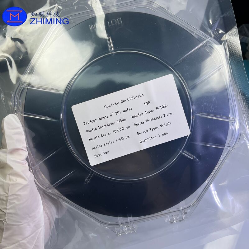
Product Information SOI (Silicon-on-Insulator) is a “sandwich” structure wafer consisting of three layers: the top silicon layer, also known as the Top Si / Device Layer, is used to fabricate transistors; the middle layer is the Buried Oxide (BOX), which provides electrical isolation; and the bottom layer is the silicon support substrate (Handle/Substrate Wafer). Compared with conventional Bulk Si wafers, SOI wafers feature complete dielectric isolation, enabling lower